
Product Info


LPWA Module Series
BG95 Hardware Design
BG95_Hardware_Design 31 / 88
V
IH
min = 1.2 V
V
IH
max = 2.0 V
When it is in low
voltage level, the
module can enter
airplane mode.
If unused, keep this
pin open.
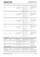
AP_READY* 19 DI
Application
processor sleep
state detection
V
IL
min = -0.3 V
V
IL
max = 0.6 V
V
IH
min = 1.2 V
V
IH
max = 2.0 V
1.8 V power domain.
If unused, keep this
pin open.
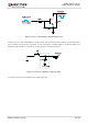
USB_BOOT 75 DI
Force the
module into
emergency
download mode
V
IL
min = -0.3 V
V
IL
max = 0.6 V
V
IH
min = 1.2 V
V
IH
max = 2.0 V
1.8 V power domain.
If unused, keep this
pin open.
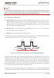
PON_TRIG 96 DI
Wake up the
module from
PSM
1.8 V power domain.
Rising-edge
triggered.
Pulled-down by
default.
If unused, keep this
pin open.
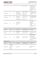
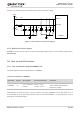
GRFC Interfaces
Pin Name Pin No. I/O Description DC Characteristics Comment
GRFC1 83 DO
Generic RF
controller
V
OL
max = 0.45 V
V
OH
min = 1.35 V
1.8 V power domain.
If unused, keep this
pin open.
GRFC2 84 DO
Generic RF
controller
V
OL
max = 0.45 V
V
OH
min = 1.35 V
BOOT_CONFIG.
Do not pull it up
before startup.
1.8 V power domain.
If unused, keep this
pin open.
RESERVED Pins
Pin Name Pin No. I/O Description DC Characteristics Comment
RESERVED
11–14, 16,
51, 56, 57,
63, 76–78,
92–95,
97–99
Reserved
Keep these pins
open.