
Product Info


LPWA Module Series
BG95 Hardware Design
BG95_Hardware_Design 30 / 88
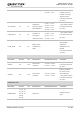
GPIO5 66 IO
General-purpose
input/output
V
OL
max = 0.45 V
V
OH
min = 1.35 V
V
IL
min = -0.3 V
V
IL
max = 0.6 V
V
IH
min = 1.2 V
V
IH
max = 2.0 V
1.8 V power domain.
If unused, keep this
pin open.
GPIO6 85 IO
General-purpose
input/output
V
OL
max = 0.45 V
V
OH
min = 1.35 V
V
IL
min = -0.3 V
V
IL
max = 0.6 V
V
IH
min = 1.2 V
V
IH
max = 2.0 V
1.8 V power domain.
If unused, keep this
pin open.
GPIO7 86 IO
General-purpose
input/output
V
OL
max = 0.45 V
V
OH
min = 1.35 V
V
IL
min = -0.3 V
V
IL
max = 0.6 V
V
IH
min = 1.2 V
V
IH
max = 2.0 V
1.8 V power domain.
If unused, keep this
pin open.
GPIO8 87 IO
General-purpose
input/output
V
OL
max = 0.45 V
V
OH
min = 1.35 V
V
IL
min = -0.3 V
V
IL
max = 0.6 V
V
IH
min = 1.2 V
V
IH
max = 2.0 V
1.8 V power domain.
If unused, keep this
pin open.
GPIO9 88 IO
General-purpose
input/output
V
OL
max = 0.45 V
V
OH
min = 1.35 V
V
IL
min = -0.3 V
V
IL
max = 0.6 V
V
IH
min = 1.2 V
V
IH
max = 2.0 V
1.8 V power domain.
If unused, keep this
pin open.
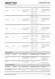
ADC Interfaces
Pin Name Pin No. I/O Description DC Characteristics Comment
ADC0 24 AI
General-purpose
ADC interface
Voltage range:
0.1–1.8 V
ADC0 and ADC1
cannot be used
simultaneously.
If unused, keep
these pins open.
ADC1 2 AI
General-purpose
ADC interface
Voltage range:
0.1–1.8 V
Other Interface Pins
Pin Name Pin No. I/O Description DC Characteristics Comment
W_DISABLE#* 18 DI
Airplane mode
control
V
IL
min = -0.3 V
V
IL
max = 0.6 V
1.8 V power domain.
Pulled up by default.