
Product Info


LPWA Module Series
BG95 Hardware Design
BG95_Hardware_Design 24 / 88
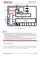
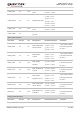
1. ADC0 and ADC1 cannot be used simultaneously, as ADC1 is connected directly to ADC0 inside the
module. The module supports use of only one ADC interface at a time: either ADC0 or ADC1.
2. PWRKEY output voltage is 1.5 V because of the voltage drop inside the Qualcomm chipset. Due to
platform limitations, the chipset has integrated the reset function into PWRKEY. Therefore, PWRKEY
should never be pulled down to GND permanently.
3. RESET_N is connected directly to PWRKEY inside the module.
4. GNSS_TXD (pin 27) and GRFC2 (pin 84) are BOOT_CONFIG pins. They should not be pulled up
before startup.
5. BG95-M4 does not support GRFC interfaces.
6. Keep all RESERVED pins and unused pins unconnected.
7. GND pins should be connected to ground in the design.
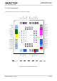
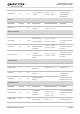
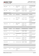
3.2. Pin Description
The following tables show the pin definition and description of BG95.
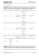
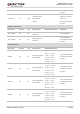
Table 4: Definition of I/O Parameters
Type Description
AI Analog Input
AO Analog Output
DI Digital Input
DO Digital Output
IO Bidirectional
PI Power Input
PO Power Output
NOTES