
Product Info


LPWA Module Series
BG95 Hardware Design
BG95_Hardware_Design 21 / 88
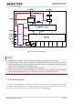
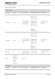
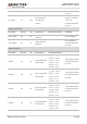
Figure 1: Functional Diagram
1. eSIM function is optional. If eSIM is selected, then any external (U)SIM cannot be used.
2. PWRKEY output voltage is 1.5 V because of the voltage drop inside the Qualcomm chipset. Due to
platform limitations, the chipset has integrated the reset function into PWRKEY. Therefore, PWRKEY
should never be pulled down to GND permanently.
3. RESET_N is connected directly to PWRKEY inside the module.
4. ADC0 and ADC1 cannot be used simultaneously, as ADC1 is connected directly to ADC0 inside the
module. BG95 supports use of only one ADC interface at a time: either ADC0 or ADC1.
2.4. Evaluation Board
In order to facilitate application development with BG95 conveniently, Quectel supplies the evaluation
board (EVB), USB to RS-232 converter cable, USB data cable, earphone, antenna and other peripherals
to control or test the module. For more details, please refer to document [1].
NOTES