
Product Info

Smart LTE Module Series
SC650T Hardware Design
SC650T_Hardware_Design 30 / 131
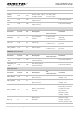
TP0_I2C_
SDA
206
OD
I2C data signal of
touch panel (TP0)
1.8V power domain.
TP1_RST
136
DO
Reset signal of
touch panel (TP1)
V
OL
max=0.45V
V
OH
min=1.35V
1.8V power domain.
Active low.
TP1_INT
137
DI
Interrupt signal of
touch panel (TP1)
V
IL
max=0.63V
V
IH
min=1.17V
1.8V power domain.
TP1_I2C_
SDA
204
OD
I2C data signal of
touch panel (TP1)
1.8V power domain.
TP1_I2C_
SCL
205
OD
I2C clock signal of
touch panel (TP1)
1.8V power domain.
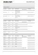
LCM Interfaces
Pin Name
Pin No.
I/O
Description
DC
Characteristics
Comment
LCD_BIAS_P
21
PO
LCD positive bias
voltage.
LCD_BIAS_N
22
AI
LCD negative bias
voltage.
WLED_EN
158
DO
LCD enable for
backlight.
WLED_PWM
30
DO
PWM signal output
LCD0_RST
127
DO
LCD0 reset signal
V
OL
max=0.45V
V
OH
min=1.35V
1.8V power domain.
Active low.
LCD0_TE
126
DI
LCD0 tearing effect
signal
V
IL
max=0.63V
V
IH
min=1.17V
1.8V power domain.
LCD1_RST
113
DO
LCD1 reset signal
V
OL
max=0.45V
V
OH
min=1.35V
1.8V power domain.
Active low.
LCD1_TE
114
DI
LCD1 tearing effect
signal
V
IL
max=0.63V
V
IH
min=1.17V
1.8V power domain.
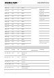
DSI0_CLK_N
116
AO
LCD0 MIPI clock
signal (negative)
DSI0_CLK_P
115
AO
LCD0 MIPI clock
signal (positive)
DSI0_LN0_N
118
AO
LCD0 MIPI lane 0
data signal
(negative)
DSI0_LN0_P
117
AO
LCD0 MIPI lane 0
data signal
(positive)
DSI0_LN1_N
120
AO
LCD0 MIPI lane 1
data signal
(negative)