
Product Info

Smart LTE Module Series
SC650T Hardware Design
SC650T_Hardware_Design 22 / 131
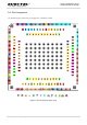
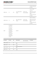
3.3. Pin Description
Table 4: I/O Parameters Definition
Type
Description
IO
Bidirectional
DI
Digital input
DO
Digital output
PI
Power input
PO
Power output
AI
Analog input
AO
Analog output
OD
Open drain
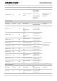
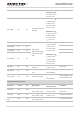
The following tables show the SC650T’s pin definition and electrical characteristics.
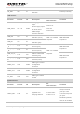
Table 5: Pin Description
Power Supply
Pin Name
Pin No.
I/O
Description
DC
Characteristics
Comment
VBAT
36,37,38
PI/PO
Power supply for the
battery.
Vmax=4.4V
Vmin=3.55V
Vnorm=3.8V
It must be able to
provide sufficient
current up to 3.0A.
It is suggested to
use a TVS to
increase voltage
surge withstand
capability.
VDD_RF
1,2
PO
Connect to external
bypass capacitors to
eliminate voltage
fluctuation of RF
part.
Vmax=4.4V
Vmin=3.55V
Vnorm=3.8V
Do not load
externally.
VPH_PWR
220,221
PO
Power supply for the
Vmax=4.4V
Peripheral power