
Product Info

Smart Module Series
SC600Y&SC600T Hardware Design
SC600Y&SC600T_Hardware_Design 105 / 134
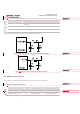
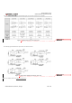
Figure 36: Coplanar Waveguide Design on a 4-layer PCB (Layer 3 as Reference Ground)
Figure 37: Coplanar Waveguide Design on a 4-layer PCB (Layer 4 as Reference Ground)
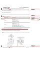
In order to ensure RF performance and reliability, the following principles should be complied
with in RF layout design:
Use an impedance simulation tool to accurately control the characteristic impedance of RF
traces to 50Ω.
The GND pins adjacent to RF pins should not be designed as thermal relief pins, and should
be fully connected to ground.
The distance between the RF pins and the RF connector should be as short as possible, and