
Product Info

Smart Module Series
SC600Y&SC600T Hardware Design
SC600Y&SC600T_Hardware_Design 104 / 134
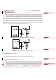
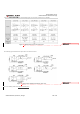
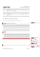
Reference Design of RF Layout
For user’s PCB, the characteristic impedance of all RF traces should be controlled to 50Ω. The
impedance of the RF traces is usually determined by the trace width (W), the materials’ dielectric
constant, the height from the reference ground to the signal layer (H), and the space between RF
traces and grounds (S). Microstrip or coplanar waveguide is typically used in RF layout to control
characteristic impedance. The following are reference designs of microstrip or coplanar waveguide
with different PCB structures.
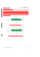
Figure 34: Microstrip Design on a 2-layer PCB
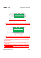
Figure 35: Coplanar Waveguide Design on a 2-layer PCB