
Product Info

Smart Module Series
SC600Y&SC600T Hardware Design
SC600Y&SC600T_Hardware_Design 48 / 134
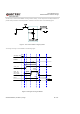
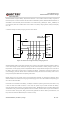
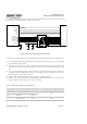
The following is a reference design for USB Type-C interface:
USB_DP
100nF
Module
C14
Switch
C2
C3
C4
C5
A0+
A0-
A1+
A0-
B0+
B0-
B1+
B1-
C0+
C0-
C1+
C1-
SEL
PD
USB_SS_TX_P
USB_SS_TX_M
USB_SS_RX_P
USB_SS_RX_M
USB_SS_SEL
R2
VDD
4.7uF
C1
VDD_3V
TX1+
TX1-
VUSB_ VBUS
CC
1
D+
D-
RX1-
RX1+
CC2
CC1
CC2
TX2+
TX2-
RX2+
RX2-
USB Type-C
C6
C7
C8
C9
C10
C11
C12
C13
USB_DM
USB_ VBUS
R1
NM
USB_OPT
Figure 13: USB Type-C Interface Reference Design
In order to ensure USB performance, please follow the following principles while designing USB interface.
It is important to route the USB signal traces as differential pairs with total grounding. The impedance
of USB differential trace is 90Ω.
Pay attention to the influence of junction capacitance of ESD protection devices on USB data lines.
Typically, the capacitance value should be less than 2pF for USB 2.0 and less than 0.5pF for USB
3.0.
Do not route signal traces under crystals, oscillators, magnetic devices and RF signal traces. It is
important to route the USB differential traces in inner-layer with ground shielding on not only upper
and lower layers but also right and left sides.
Keep the ESD protection devices as close as possible to the USB connector.
Make sure the trace length difference between USB 2.0 DM/DP differential pair and that between
USB 3.0 RX/TX differential pairs both do not exceed 0.7mm.
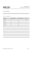
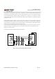
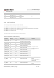
Table 11: USB Trace Length Inside the Module
Pin No. Signal Length (mm) Length Difference (DP-DM)
33 USB_DM 39.52
-0.45
32 USB_DP 39.07
171 USB_SS_RX_P 28.55 0.32