
Product Info


LPWA Module Series
BG95-M3 Mini PCIe Hardware Design
BG95-M3_Mini_PCIe_Hardware_Design 39 / 53
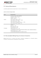
Table 22: 3.3 V Digital I/O Characteristics
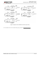
Table 23: 1.8 V Digital I/O Characteristics
1. The PCM and I2C interfaces belong to 1.8 V power domain and other I/O interfaces belong to
VCC_3V3 power domain.
2. The maximum voltage value of V
IL
for PERST# and W_DISABLE# is 0.5 V.
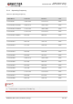
6.4. RF Characteristics
The following tables show the conducted RF output power and receiving sensitivity of the module.
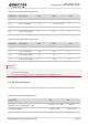
Table 24: Conducted RF Output Power
Parameter Description Min. Max. Unit
V
IH
Input High Voltage 0.7 × VCC_3V3 VCC_3V3 + 0.3 V
V
IL
Input Low Voltage -0.3 0.3 × VCC_3V3 V
V
OH
Output High Voltage VCC_3V3 - 0.5 VCC_3V3 V
V
OL
Output Low Voltage 0 0.4 V
Parameter Description Min. Max. Unit
V
IH
Input High Voltage 1.2 2.0 V
V
IL
Input Low Voltage -0.3 0.6 V
V
OH
Output High Voltage 1.35 1.8 V
V
OL
Output Low Voltage 0 0.45 V
Frequency Max. Min.
LTE-FDD B1/B2/B3/B4/B5/B8/B12/B13/B18/B19/B20/
B25/B26
1)
/B27
1)
/B28/B66/B71
2)
/B85
21 dBm + 1.7/-3 dB < -39 dBm
GSM850/EGSM900 33 dBm ± 2 dB 5 dBm ± 5 dB
NOTES