
Product Info


LPWA Module Series
BG95-M3 Mini PCIe Hardware Design
BG95-M3_Mini_PCIe_Hardware_Design 23 / 53
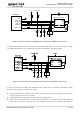
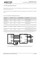
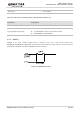
Figure 6: Reference Design of USB Interface
A common mode choke L1 is recommended to be added in series between the module and the MCU in
order to suppress EMI spurious transmission. Meanwhile, the 0 Ω resistors (R3 and R4) should be added
in series between the module and the test points so as to facilitate debugging, and the resistors are not
mounted by default. In order to ensure the integrity of USB data line signal, L1/R3/R4 must be placed
close to the module, and also the resistors should be placed close to each other. The extra stubs of trace
must be as short as possible.
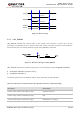
The following principles should be complied with when design the USB interface, so as to meet USB 2.0
specification.
It is important to route the USB signal traces as differential pairs with ground surrounded. The
impedance of USB differential trace is 90 Ω.
Do not route signal traces under crystals, oscillators, magnetic devices and RF signal traces. It is
important to route the USB differential traces in inner-layer of the PCB, and surround the traces with
ground on that layer and with ground planes above and below.
Junction capacitance of the ESD protection device might cause influences on USB data lines, so
please pay attention to the selection of the device. Typically, the stray capacitance should be less
than 2 pF.
Keep the ESD protection devices as close to the USB connector as possible.
BG95-M3 Mini PCIe can only be used as a slave device.
NOTE