
Product Info


LPWA Module Series
BG95-M3 Mini PCIe Hardware Design
BG95-M3_Mini_PCIe_Hardware_Design 22 / 53
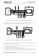
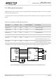
capacitor between USIM_VDD and GND should be not more than 1 μF and be placed close to the
(U)SIM card connector.
To avoid cross-talk between USIM_DATA and USIM_CLK, keep them away from each other and
shield them with surrounded ground.
In order to offer good ESD protection, it is recommended to add a TVS diode with parasitic
capacitance not exceeding 15 pF. The 0 Ω resistors should be added in series between the module
and the (U)SIM card connector so as to facilitate debugging. The 33 pF capacitors are used for
filtering interference of EGSM900. Please note that the (U)SIM peripheral circuit should be close to
the (U)SIM card connector.
The pull-up resistor on USIM_DATA line can improve anti-jamming capability when long layout trace
and sensitive occasion are applied, and should be placed close to the (U)SIM card connector.
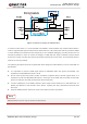
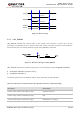
3.4. USB Interface
The module provides one integrated Universal Serial Bus (USB) interface which complies with the USB
2.0 specification and supports operation at low-speed (1.5 Mbps) and full-speed (12 Mbps) modes. The
USB interface is used for AT command communication, data transmission, GNSS NMEA output, software
debugging, and firmware upgrade.
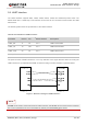
The following table shows the pin definition of USB interface.
Table: Pin Definition of USB Interface
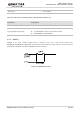
The following figure shows a reference design of USB interface.
Pin Name Pin No. I/O Description Comment
USB_DM 36 IO USB differential data (-) Require differential impedance of 90 Ω
USB_DP 38 IO USB differential data (+) Require differential impedance of 90 Ω