
Product Info


LPWA Module Series
BG95-M3 Mini PCIe Hardware Design
BG95-M3_Mini_PCIe_Hardware_Design 21 / 53
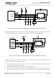
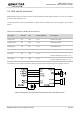
USIM_VDD
GND
USIM_RST
USIM_CLK
USIM_DATA
USIM_DET
100 nF
GND
GND
33 pF 33 pF 33 pF
VCC
RST
CLK
IO
VPP
GND
GND
USIM_VDD
15K
(U)SIM Card Connector
Module
1.8V
51K
0R
0R
0R
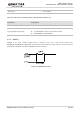
Figure 4: Reference Design of (U)SIM Interface with 8-Pin (U)SIM Card Connector
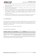
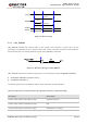
If (U)SIM card detection function is not needed, please keep USIM_DET unconnected. A reference design
of (U)SIM interface with a 6-pin (U)SIM card connector is illustrated in the following figure.
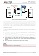
Figure 5: Reference Design of (U)SIM Interface with 6-Pin (U)SIM Card Connector
In order to enhance the reliability and availability of the (U)SIM card in customers’ applications, please
follow the criteria below in (U)SIM circuit design:
Keep the placement of (U)SIM card connector to the module as close as possible. Keep the trace
length as less than 200 mm as possible.
Keep (U)SIM card signals away from RF and power supply traces.
Assure the ground between the module and the (U)SIM card connector short and wide. Keep the
trace width of ground no less than 0.5 mm to maintain the same electric potential. The decouple