
Product Info


LPWA Module Series
BG95-M3 Mini PCIe Hardware Design
BG95-M3_Mini_PCIe_Hardware_Design 19 / 53
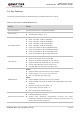
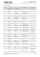
Table 5: Overview of Operating Modes
Mode Details
Normal
Operation
Idle
Software is active. The module has registered on the network, and it is
ready to send and receive data.
Talk/Data
Network connection is ongoing. In this mode, the power consumption is
decided by network setting and data transfer rate.
Minimum
Functionality
Mode
AT+CFUN=0 command can set the module to a minimum functionality mode without
removing the power supply. In this case, both RF function and (U)SIM card will be
invalid.
Airplane Mode
AT+CFUN=4 command or W_DISABLE# pin can set the module to airplane mode. In
this case, RF function will be invalid.
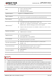
3.2. Power Supply
The following table shows the definition of VCC_3V3 pins and ground pins.
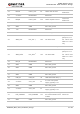
Table 6: Definition of VCC_3V3 and GND Pins
The typical supply voltage of BG95-M3 Mini PCIe is 3.3 V. In 2G network, the input peak current may
reach 2.7 A during the transmitting time. Therefore, the power supply must be able to provide a rated
current of 2.7 A at least, and a low-ESR bypass capacitor no less than 470 µF should be used to prevent
the voltage from dropping. If the switching power supply is used to supply power to the module, the power
device and power supply routing traces of the switching power supply should avoid the antennas as much
as possible to prevent EMI interference.
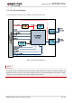
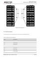
The following figure shows a reference design of power supply where R2 and R3 are 1% tolerance
resistors, and C3 is a low-ESR capacitor.
Pin Name Pin No. I/O Power Domain Description
VCC_3V3 2, 39, 41, 52 PI 3.0–3.6 V Typically 3.3 V DC supply
GND
4, 9, 15, 18, 21, 26, 27, 29, 34, 35,
37, 40, 43, 50
Mini card ground