
Product Info


LPWA Module Series
BG95-M3 Mini PCIe Hardware Design
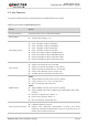
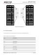
BG95-M3_Mini_PCIe_Hardware_Design 16 / 53
Table 4: Pin Description
Pin No.
Mini PCI Express
Standard Name
BG95-M3 Mini
PCIe Pin Name
I/O Description Comment
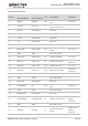
1 WAKE# WAKE# OC
Used to wake up the
host
Active low
2 3.3 Vaux VCC_3V3 PI
3.0–3.6 V DC power
supply, typically 3.3 V
3 COEX1 RESERVED Reserved
4 GND GND Mini card ground
5 COEX2 RESERVED Reserved
6 1.5V RESERVED Reserved
7 CLKREQ# RESERVED Reserved
8 UIM_PWR USIM_VDD PO
(U)SIM card power
supply
1.8 V only
9 GND GND Mini card ground
10 UIM_DATA USIM_DATA IO (U)SIM card data 1.8 V only
11 REFCLK- UART_RX DI UART receive data
Connect to
DTE’s TX.
12 UIM_CLK USIM_CLK DO (U)SIM card clock 1.8 V only
13 REFCLK+ UART_TX DO UART transmit data
Connect to
DTE’s RX.
14 UIM_RESET USIM_RST DO (U)SIM card reset 1.8 V only
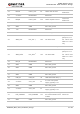
15 GND GND Mini card ground
16 UIM_VPP RESERVED Reserved
17 RESERVED RI DO
Used to wake up the
host
Active low
18 GND GND Mini card ground
19 RESERVED RESERVED Reserved
20 W_DISABLE# W_DISABLE# DI Airplane mode control
Pulled up by
default.
Active low.
21 GND GND
Mini card ground
22 PERST# PERST# DI
Fundamental reset
signal
Pulled up by
default.
Active low.