
Product Info

LTE Standard Module Series
EG95 Hardware Design
EG95_Hardware_Design 51 / 93
3.16. ADC Interface
The module provides one analog-to-digital converter (ADC) interface. AT+QADC=0 command can be
used to read the voltage value on ADC0 pin. For more details about the command, please refer to
document [2].
In order to improve the accuracy of ADC voltage values, the traces of ADC should be surrounded by
ground.
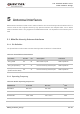
Table 19: Pin Definition of ADC Interface
Pin Name
Pin No.
I/O
Description
Comment
ADC0
24
AI
Force the module to enter
emergency download mode
If unused, keep this pin
open.
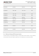
The following table describes the characteristics of ADC interface.
Table 20: Characteristics of ADC Interface
Parameter
Min.
Typ.
Max.
Unit
ADC0 Voltage Range
0.3
VBAT_BB
V
ADC Resolution
15
bits
1. It is prohibited to supply any voltage to ADC pins when ADC pins are not powered by VBAT.
2. It is recommended to use resistor divider circuit for ADC application.
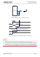
3.17. Behaviors of RI
AT+QCFG="risignaltype","physical" command can be used to configure RI behavior. The default RI
behaviors can be changed by AT+QCFG="urc/ri/ring" command. Please refer to document [2] for
details.
No matter on which port URC is presented, URC will trigger the behavior of RI pin.
NOTES