
Product Info


LTE Standard Module Series
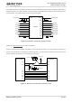
EG95 Hardware Design
EG95_Hardware_Design 48 / 93
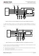
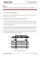
PCM_DIN
PCM_DOUT
PCM_SYNC
PCM_CLK
I2C_SCL
I2C_SDA
Module
1.8V
4.7K
4.7K
BCLK
LRCK
DAC
ADC
SCL
SDA
BIAS
MICBIAS
INP
INN
LOUTP
LOUTN
Codec
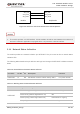
Figure 24: Reference Circuit of PCM Application with Audio Codec
1. It is recommended to reserve an RC (R=22Ω, C=22pF) circuit on the PCM lines, especially for
PCM_CLK.
2. EG95 works as a master device pertaining to I2C interface.
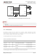
3.13. SPI Interface
SPI interface of EG95 acts as the master only. It provides a duplex, synchronous and serial
communication link with the peripheral devices. It is dedicated to one-to-one connection, without chip
select. Its operation voltage is 1.8V with clock rates up to 50MHz.
The following table shows the pin definition of SPI interface.
Table 15: Pin Definition of SPI Interface
Pin Name
Pin No.
I/O
Description
Comment
SPI_CLK
26
DO
Clock signal of SPI interface
1.8V power domain
SPI_MOSI
27
DO
Master output slave input of SPI
interface
1.8V power domain
SPI_MISO
28
DI
Master input slave output of SPI
interface
1.8V power domain
The following figure shows a reference design of SPI interface with peripherals.
NOTES