
Product Info


LTE Standard Module Series
EG95 Hardware Design
EG95_Hardware_Design 47 / 93
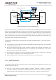
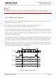
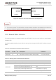
PCM_CLK
PCM_SYNC
PCM_DOUT
MSB
LSB
PCM_DIN
125us
MSB
1 2 3231
LSB
Figure 23: Auxiliary Mode Timing
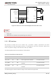
The following table shows the pin definition of PCM and I2C interfaces which can be applied on audio
codec design.
Table 14: Pin Definition of PCM and I2C Interfaces
Pin Name
Pin No.
I/O
Description
Comment
PCM_DIN
6
DI
PCM data input
1.8V power domain
PCM_DOUT
7
DO
PCM data output
1.8V power domain
PCM_SYNC
5
IO
PCM data frame
synchronization signal
1.8V power domain
PCM_CLK
4
IO
PCM data bit clock
1.8V power domain
I2C_SCL
40
OD
I2C serial clock
Require an external pull-up to
1.8V
I2C_SDA
41
OD
I2C serial data
Require an external pull-up to
1.8V
Clock and mode can be configured by AT command, and the default configuration is master mode using
short frame synchronization format with 2048KHz PCM_CLK and 8KHz PCM_SYNC. Please refer to
document [2] about AT+QDAI command for details.
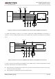
The following figure shows a reference design of PCM interface with external codec IC.