
Product Info

LTE Standard Module Series
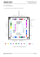
EG95 Hardware Design
EG95_Hardware_Design 26 / 93
V
IH
max=2.0V
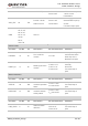
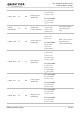
PCM Interface
Pin Name
Pin No.
I/O
Description
DC Characteristics
Comment
PCM_DIN
6
DI
PCM data input
V
IL
min=-0.3V
V
IL
max=0.6V
V
IH
min=1.2V
V
IH
max=2.0V
1.8V power domain.
If unused, keep it
open.
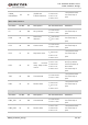
PCM_DOUT
7
DO
PCM data output
V
OL
max=0.45V
V
OH
min=1.35V
1.8V power domain.
If unused, keep it
open.
PCM_SYNC
5
IO
PCM data frame
synchronization
signal
V
OL
max=0.45V
V
OH
min=1.35V
V
IL
min=-0.3V
V
IL
max=0.6V
V
IH
min=1.2V
V
IH
max=2.0V
1.8V power domain.
In master mode, it is
an output signal. In
slave mode, it is an
input signal.
If unused, keep it
open.
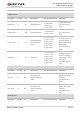
PCM_CLK
4
IO
PCM clock
V
OL
max=0.45V
V
OH
min=1.35V
V
IL
min=-0.3V
V
IL
max=0.6V
V
IH
min=1.2V
V
IH
max=2.0V
1.8V power domain.
In master mode, it is
an output signal. In
slave mode, it is an
input signal.
If unused, keep it
open.
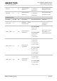
I2C Interface
Pin Name
Pin No.
I/O
Description
DC Characteristics
Comment
I2C_SCL
40
OD
I2C serial clock.
Used for external
codec
An external pull-up
resistor is required.
1.8V only.
If unused, keep it
open.
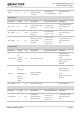
I2C_SDA
41
OD
I2C serial data.
Used for external
codec
An external pull-up
resistor is required.
1.8V only.
If unused, keep it
open.
ADC Interface
Pin Name
Pin No.
I/O
Description
DC Characteristics
Comment