
Product Info

LTE Standard Module Series
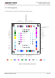
EG95 Hardware Design
EG95_Hardware_Design 21 / 93
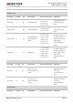
1.
1)
PWRKEY output voltage is 0.8V because of the diode drop in the Qualcomm chipset.
2. Keep all RESERVED pins and unused pins unconnected.
3. GND pads should be connected to ground in the design.
4. Please note that the definition of pin 49 and 56 are different among EG95-E and EG95-NA/-EX/-NAX.
For more details, please refer to Table 4.
3.3. Pin Description
The following tables show the pin definition and description of EG95.
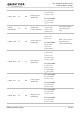
Table 3: IO Parameters Definition
Type
Description
AI
Analog Input
AO
Analog Output
DI
Digital Input
DO
Digital Output
IO
Bidirectional
OD
Open Drain
PI
Power Input
PO
Power Output
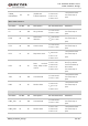
Table 4: Pin Description
Power Supply
Pin Name
Pin No.
I/O
Description
DC
Characteristics
Comment
VBAT_BB
32, 33
PI
Power supply for
module’s
baseband part
Vmax=4.3V
Vmin=3.3V
Vnorm=3.8V
It must be provided with
sufficient current up to
0.8A.
VBAT_RF
52, 53
PI
Power supply for
Vmax=4.3V
It must be provided with
NOTES