
Product Info


LTE-A Module Series
EG12 Hardware Design
EG12_Hardware_Design 55 / 100
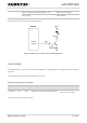
PCM_IN
PCM_OUT
PCM_SYNC
PCM_CLK
I2C_SCL
I2C_SDA
Module
1.8V
4.7K
4.7K
BCLK
LRCK
DAC
ADC
SCL
SDA
BIAS
MICBIAS
INP
INN
LOUTP
LOUTN
Codec
Figure 26: Reference Circuit of PCM Application with Audio Codec
1. It is recommended to reserve an RC (R=22Ω, C=22pF) circuit on the PCM lines, especially for
PCM_CLK.
2. EG12 works as a master device pertaining to I2C interface.
3.14. ADC Interfaces
The module provides two Analog-to-Digital Converters (ADC) interfaces. AT+QADC=0 command can be
executed to read the voltage value on ADC0. AT+QADC=1 command can be executed to read the
voltage value on ADC1 pin. For more details about these AT+QADC commands, please refer to
document [2].
In order to improve the accuracy of ADC, the trace of ADC should be surrounded by ground.
Table 19: Pin Definition of the ADC Interfaces
The following table describes characteristics of ADC interfaces.
Pin Name
Pin No.
Description
ADC0
173
General purpose analog to digital converter interface.
If unused, keep it open.
ADC1
175
General purpose analog to digital converter interface
If unused, keep it open.
NOTES