
Product Info


LTE-A Module Series
EG12 Hardware Design
EG12_Hardware_Design 54 / 100
The following table shows the pin definition of PCM interface and I2C interface, both of which can be
applied on audio codec design.
Table 18: Pin Definition of PCM interface and I2C Interface
Clock and mode can be configured by AT command, and the default configuration is master mode using
short frame synchronization format with 2048kHz PCM_CLK and 8kHz PCM_SYNC. Please refer to
document [2] for details about AT+QDAI command.
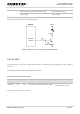
The following figure shows a reference design of PCM interface with an external codec IC.
Pin Name
Pin No.
I/O
Description
Comment
PCM_IN
66
DI
PCM data input
1.8V power domain.
If unused, keep it open.
PCM_OUT
68
DO
PCM data output
1.8V power domain.
If unused, keep it open.
PCM_SYNC
65
IO
PCM data frame
synchronization
signal
1.8V power domain.
In master mode, it is an output signal.
In slave mode, it is an input signal.
If unused, keep it open.
PCM_CLK
67
IO
PCM data clock
1.8V power domain.
In master mode, it is an output signal.
In slave mode, it is an input signal.
If unused, keep it open.
I2C_SDA
42
OD
I2C serial data
An external pull-up resistor is required.
If unused, keep it open.
I2C_SCL
43
OD
I2C serial clock
An external pull-up resistor is required.
If unused, keep it open.
I2S_MCLK
152
DO
Clock output
Provide a digital clock output for an
external audio codec.
If unused, keep it open.