
Product Info


LTE-A Module Series
EG12 Hardware Design
EG12_Hardware_Design 51 / 100
MCU/ARM
TXD
RXD
VDD_EXT
10K
VCC_MCU
4.7K
10K
VDD_EXT
TXD
RXD
RTS
CTS
DTR
RI
RTS
CTS
GND
GPIO DCD
Module
GPIO
EINT
VDD_EXT
4.7K
GND
1nF
1nF
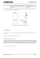
Figure 22: Level Translation Reference Circuit with MOSFETs
Transistor circuit solution is not suitable for applications with high baud rates exceeding 460Kbps.
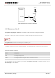
3.12. SPI Interface
EG12 provides one SPI interface multiplexed from BT UART interface. The interface only supports master
mode with a maximum clock frequency up to 50MHz. The following table shows the pin definition of SPI
interface.
Table 16: Pin Definition of SPI Interface
The following figure shows the timing relationship of SPI interface.
Pin Name
Pin No.
I/O
Description
Comment
BT_TXD
163
DO
Can be multiplexed into SPI_MOSI.
1.8V power domain
BT_CTS
164
DO
Can be multiplexed into SPI_CLK.
BT_RXD
165
DI
Can be multiplexed into SPI_MISO.
BT_RTS
166
DI
Can be multiplexed into SPI_CS.
NOTE