
Product Info


LTE-A Module Series
EG12 Hardware Design
EG12_Hardware_Design 47 / 100
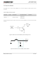
USB_DP
USB_DM
GND
USB_DP
USB_DM
GND
R1
R2
Close to Module
R3
R4
Test Points
ESD Array
NM_0R
NM_0R
0R
0R
Minimize these stubs
Module
Host
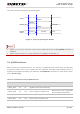
USB_VBUS
VDD
USB_SS_TX_P
USB_SS_TX_M
USB_SS_RX_P
USB_SS_RX_M
C1
C3
C4
100nF
100nF
100nF
100nF
USB_SS_RX_P
USB_SS_RX_M
USB_SS_TX_P
USB_SS_TX_M
USB_ID GPIO
C2
Figure 20: Reference Circuit of USB Application
In order to ensure the signal integrity of USB data lines, C1, and C2 have been already installed in the
module; C3 and C4 must be placed close to the host; and R1~R4 should be placed close to each other.
The extra stubs of trace must be as short as possible.
The following principles of USB interface should be complied with, so as to meet USB 2.0 & USB 3.0
specifications.
It is important to route the USB 2.0 & 3.0 signal traces as differential pairs with total grounding. The
impedance of USB differential trace is 90Ω.
For USB 2.0 signal traces, the trace length should be less than 120mm, and the differential data pair
matching should be less than 2mm (15ps).
For USB 3.0 signal traces, the maximum length of each differential data pair (TX/RX) is
recommended to be less than 100mm, and each differential data pair matching should be less than
0.7mm (5ps).
Do not route signal traces under crystals, oscillators, magnetic devices, PCIe and RF signal traces. It
is important to route the USB differential traces in inner-layer with ground shielding on not only upper
and lower layers but also right and left sides.
If a USB connector is used, please keep the ESD protection components as close to the USB
connector as possible. Pay attention to the influence of junction capacitance of ESD protection
components on USB data lines. Typically, the capacitance value should be less than 2.0pF for USB