
Product Info


LTE-A Module Series
EG12 Hardware Design
EG12_Hardware_Design 37 / 100
3.6.2. Decrease Voltage Drop
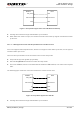
The power supply range of the module is from 3.3V to 4.3V. Please make sure the input voltage will never
drop below 3.3V. The following figure shows the voltage drop during Tx power in 3G and 4G networks.
VCC
Burst
Transmission
Min. 3.3V
Ripple
Drop
Burst
Transmission
Figure 8: Power Supply Limits during Tx Power
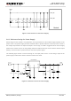
To decrease voltage drop, a bypass capacitor of about 100µF with low ESR should be used, and a
multi-layer ceramic chip (MLCC) capacitor array should also be reserved due to its ultra-low ESR. It is
recommended to use three ceramic capacitors (100nF, 33pF, 10pF) for composing the MLCC array, and
place these capacitors close to VBAT pins. The main power supply from an external application has to be
a single voltage source and can be expanded to two sub paths with star structure. The width of VBAT_BB
trace should be no less than 1mm; and the width of VBAT_RF trace should be no less than 2mm. In
principle, the longer the VBAT trace is, the wider it should be.
In addition, in order to get a stable power source, it is suggested to use a zener diode of which reverse
zener voltage is 5.1V and dissipation power is more than 0.5W. The following figure shows the star
structure of the power supply.
92~94, 96~100,
102~106, 108~112,
114~118, 120~126,
128~133, 141, 142, 148,
153, 154, 157, 158, 167,
174, 177, 178, 181, 184,
187, 191, 196, 202~208,
214~299