
Product Info


LTE-A Module Series
EG12 Hardware Design
EG12_Hardware_Design 26 / 100
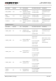
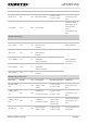
DCD
59
DO
Data carrier
detection
V
OL
max=0.45V
V
OH
min=1.35V
1.8V power domain.
If unused, keep it
open.
TXD
60
DO
Transmit data
V
OL
max=0.45V
V
OH
min=1.35V
1.8V power domain.
If unused, keep it
open.
RI
61
DO
Ring indication
V
OL
max=0.45V
V
OH
min=1.35V
1.8V power domain.
If unused, keep it
open.
DTR
62
DI
Data terminal
ready, sleep mode
control
V
IL
min=-0.3V
V
IL
max=0.6V
V
IH
min=1.2V
V
IH
max=2.0V
1.8V power domain.
Pulled up by
default. Pulling
down to low level
will wake up the
module.
If unused, keep it
open.
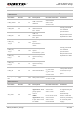
Debug UART Interface
Pin Name
Pin No.
I/O
Description
DC Characteristics
Comment
DBG_RXD
136
DI
Receive data
V
IL
min=-0.3V
V
IL
max=0.6V
V
IH
min=1.2V
V
IH
max=2.0V
1.8V power domain.
If unused, keep it
open.
DBG_TXD
137
DO
Transmit data
V
OL
max=0.45V
V
OH
min=1.35V
1.8V power domain.
If unused, keep it
open.
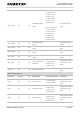
BT UART Interface (Can be multiplexed into SPI interface)
Pin Name
Pin No.
I/O
Description
DC Characteristics
Comment
BT_EN
3
DO
BT function enable
control
V
OL
max=0.45V
V
OH
min=1.35V
1.8V power domain.
If unused, keep it
open.
BT_TXD
163
DO
Transmit data
V
OL
max=0.45V
V
OH
min=1.35V
1.8V power domain.
If unused, keep it
open.
BT UART interface
pin by default.
Can be multiplexed
into SPI_MOSI.
BT_CTS
164
DO
Clear to send
V
OL
max=0.45V
V
OH
min=1.35V
1.8V power domain.
If unused, keep it
open.