
Product Info

LTE Standard Module Series
EC21 Mini PCIe Hardware Design
EC21_Mini_PCIe_Hardware_Design 61 / 64
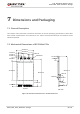
Do not apply solder mask on the PCB area where the module is mounted, so as to ensure better heat
dissipation performance.
The reference ground of the area where the module is mounted should be complete, and add ground
vias as many as possible for better heat dissipation.
Add a heatsink on the top of the module and the heatsink should be designed with as many fins as
possible to increase heat dissipation area. Meanwhile, a thermal pad with high thermal conductivity
should be used between the heatsink and module.
Add a thermal pad with appropriate thickness at the bottom of the module to conduct the heat to
PCB.
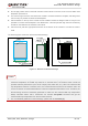
The following figure shows the referenced heatsink design.
Figure 17: Referenced Heatsink Design
1. The module offers the best performance when the internal BB chip stays below 105°C. When the
maximum temperature of the BB chip reaches or exceeds 105°C, the module works normal but
provides reduced performance (such as RF output power, data rate, etc.). When the maximum BB
chip temperature reaches or exceeds 115°C, the module will disconnect from the network, and it will
recover to network connected state after the maximum temperature falls below 115°C. Therefore, the
thermal design should be maximally optimized to make sure the maximum BB chip temperature
always maintains below 105°C. Customers can execute AT+QTEMP command and get the
maximum BB chip temperature from the first returned value.
2. For more detailed guidelines on thermal design, please refer to document [4].
NOTES