
Product Info


LTE Standard Module Series
EC21 Mini PCIe Hardware Design
EC21_Mini_PCIe_Hardware_Design 32 / 64
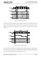
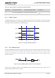
The following figure shows a reference design of PCM interface with an external codec IC.
PCM_DIN
PCM_DOUT
PCM_SYNC
PCM_CLK
I2C_SCL
I2C_SDA
Codec
Module
1.8V
BCLK
FS
DACIN
ADCOUT
SCLK
SDIN
MIC_BIAS
MIC+
MIC-
SPKOUT+
SPKOUT-
Figure 9: Reference Circuit of PCM Application with Audio Codec
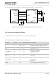
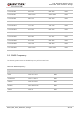
3.8. Control and Indicator Signals
The following table shows the pin definition of control and indicator signals.
Table 10: Pin Definition of Control and Indicator Signals
Pin Name Pin No. I/O Power Domain Description
RI 17 DO 3.3V Output signal used to wake up the host
DTR 31 DI 3.3V Sleep mode control
W_DISABLE# 20 DI 3.3V
Airplane mode control;
Pulled up by default;
Active low.
PERST# 22 DI 3.3V
Fundamental reset signal;
Active low.
LED_WWAN# 42 OC
LED signal for indicating the network status
of the module;
Active low.
WAKE# 1 OC
Output signal to wake up the host