
Product Info

LTE Standard Module Series
EC21 Mini PCIe Hardware Design
EC21_Mini_PCIe_Hardware_Design 24 / 64
1. Keep all NC, reserved and unused pins unconnected.
2.
1)
The digital audio (PCM) function is only supported on Telematics version.
3.3. Power Supply
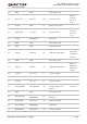
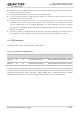
The following table shows pin definition of VCC_3V3 pins and ground pins.
Table 5: Pin Definition of VCC_3V3 and GND Pins
The typical supply voltage of EC21 Mini PCIe is 3.3V. In the 2G network, the input peak current may reach
2.7A during the transmitting time. Therefore, the power supply must be able to provide enough current,
and a bypass capacitor of no less than 470µF with low ESR should be used to prevent the voltage from
dropping.
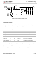
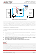
The following figure shows a reference design of power supply. The precision of resistor R2 and R3 is 1%,
and the capacitor C3 needs a low ESR.
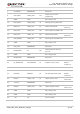
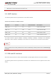
48 1.5V NC Not connected
49 RESERVED PCM_DIN
1)
DI PCM data input
50 GND GND Mini card ground
51 RESERVED PCM_SYNC
1)
IO PCM frame synchronization
52 3.3Vaux VCC_3V3 PI 3.3V DC supply
Pin Name Pin No. I/O Power Domain Description
VCC_3V3 2, 39, 41, 52 PI 3.0V~3.6V 3.3V DC supply
GND
4, 9, 15, 18, 21,
26, 27, 29, 34, 35,
37, 40, 43, 50
Mini card ground
NOTES