
Product Info

LTE Standard Module Series
EC21 Hardware Design
EC21_Hardware_Design 52 / 120
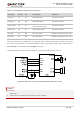
Table 10: Pin Description of USB Interface
Pin Name Pin No. I/O Description Comment
USB_DP 69 IO USB differential data bus (+)
Require differential
impedance of 90Ω
USB_DM 70 IO USB differential data bus (-)
Require differential
impedance of 90Ω
USB_VBUS 71 PI
USB power supply,
used for USB detection
Typical 5.0V
GND 72 Ground
For more details about the USB 2.0 specifications, please visit http://www.usb.org/home
.
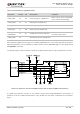
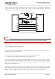
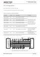
The USB interface is recommended to be reserved for firmware upgrade in customers’ designs. The
following figure shows a reference circuit of USB interface.
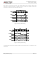
Figure 19: Reference Circuit of USB Application
A common mode choke L1 is recommended to be added in series between the module and customer’s
MCU in order to suppress EMI spurious transmission. Meanwhile, the 0Ω resistors (R3 and R4) should be
added in series between the module and the test points so as to facilitate debugging, and the resistors are
not mounted by default. In order to ensure the integrity of USB data line signal, L1/R3/R4 components
must be placed close to the module, and also these resistors should be placed close to each other. The
extra stubs of trace must be as short as possible.
The following principles should be complied with when design the USB interface, so as to meet USB 2.0
specification.
It is important to route the USB signal traces as differential pairs with total grounding. The impedance
of USB differential trace is 90Ω.