
Product Info

LTE Standard Module Series
EC21 Hardware Design
EC21_Hardware_Design 26 / 120
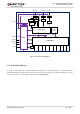
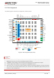
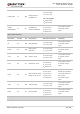
5. Pins 119~126 and 128 are used for SGMII interface.
6. Pins 24~27 for PCM function are multiplexing pins used for audio design on EC21 module and BT
function on FC20 module.
7. SD card, wireless connectivity and SGMII interfaces (pins 37~40, 118, 127, 129~139, 119~126, 128,
23, 28~34) are not supported on ThreadX module.
8. Keep all RESERVED pins and unused pins unconnected.
9. GND pads 85~112 should be connected to ground in the design. RESERVED pads 73~84 should not
be designed in schematic and PCB decal, and these pins should be served as a keepout area.
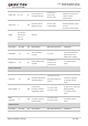
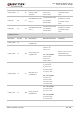
3.3. Pin Description
The following tables show the pin definition of EC21 module.
Table 3: I/O Parameters Definition
Type Description
AI Analog Input
AO Analog Output
DI Digital Input
DO Digital Output
IO Bidirectional
OD Open Drain
PI Power Input
PO Power Output
Table 4: Pin Description
Power Supply
Pin Name Pin No. I/O Description DC Characteristics Comment
VBAT_BB 59, 60 PI
Power supply for
module’s baseband
part
Vmax=4.3V
Vmin=3.3V
Vnorm=3.8V
It must be provided with
sufficient current up to
0.8A.