
Product Info

LPWA Module Series
BC66-NA Hardware Design
BC66-NA_Hardware_Design 44 / 59
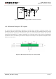
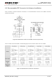
Use impedance simulation tool to control the characteristic impedance of RF traces as 50Ω.
The GND pins adjacent to RF pins should not be designed as thermal relief pads, and should be fully
connected to ground.
The distance between the RF pins and the RF connector should be as short as possible, and all the
right angle traces should be changed to curved ones.
There should be clearance area under the signal pin of the antenna connector or solder joint.
The reference ground of RF traces should be complete. Meanwhile, adding some ground vias around
RF traces and the reference ground could help to improve RF performance. The distance between
the ground vias and RF traces should be no less than two times the width of RF signal traces (2*W).
For more details, please refer to document [2].
4.5. Antenna Requirements
To minimize the loss on RF trace and RF cable, please pay attention to the antenna design. The following
tables show the requirements on NB-IoT antenna.
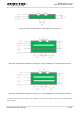
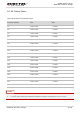
Table 17: Antenna Cable Insertion Loss Requirements
Band Requirements
LTE B5/B8/B12/B13/B17/B18/B19/B20/B26/B28/B71/B85 Cable Insertion loss: <1dB
LTE B1/B2/B3/B4/B25/B66 Cable Insertion loss: <1.5dB
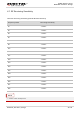
Table 18: Required Antenna Parameters
Parameters Requirements
Frequency Range 617MHz~2200MHz
VSWR ≤2
Efficiency > 30%
Max Input Power (W) 50
Input Impedance (Ω) 50