
Product Info

LPWA Module Series
BC66-NA Hardware Design
BC66-NA_Hardware_Design 43 / 59
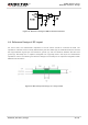
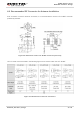
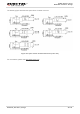
Figure 27: Coplanar Waveguide Line Design on a 2-layer PCB
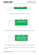
Figure 28: Coplanar Waveguide Line Design on a 4-layer PCB (Layer 3 as Reference Ground)
Figure 29: Coplanar Waveguide Line Design on a 4-layer PCB (Layer 4 as Reference Ground)
In order to ensure RF performance and reliability, the following principles should be complied with in RF
layout design: