
Product Info


LPWA Module Series
BC66-NA Hardware Design
BC66-NA_Hardware_Design 38 / 59
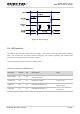
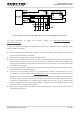
3.11. ADC Interface*
The module provides a 10-bit ADC input channel to read the voltage value. The interface is available in
active mode, and has to be woken up first to ensure availability in sleep modes.
Table 12: Pin Definition of ADC Interface
“*” means under development.
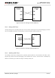
3.12. RI Behaviors
When there is a message received or URC output, the module will notify DTE through RI pin.
Table 13: RI Signal Status
Module Status RI Signal Level
Idle RI keeps in high level
SMS
When an SMS is received, RI outputs 120ms low pulse first and then changes to
high level and starts data output.
URC
When URC is incoming, RI outputs 120ms low pulse first and then changes to
high level and starts data output.
Pin Name Pin No. Description Sample Range
ADC0* 9 Analog to digital converter interface 0V ~ 1.4V
NOTE