
Product Info

LPWA Module Series
BC66-NA Hardware Design
BC66-NA_Hardware_Design 19 / 59
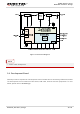
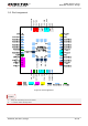
3.3. Pin Description
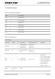
Table 3: I/O Parameters Definition
Type Description
AI Analog input
AO Analog output
DI Digital input
DO Digital output
IO Bidirectional
PI Power input
PO Power output
Table 4: Pin Description
Power Supply
Pin Name Pin No. I/O Description DC Characteristics Comment
VBAT_BB 42 PI
Power supply for
the module’s
baseband part
Vmax=3.63V
Vmin=2.1V
Vnorm=3.3V
VBAT_RF 43 PI
Power supply for
the module’s RF
part
Vmax=3.63V
Vmin=2.1V
Vnorm=3.3V
VDD_
EXT
24 PO
1.8V output
power supply
Vnorm=1.8V
No voltage output in
PSM mode.
It is intended to supply
power for the module’s
pull-up circuits, and is
thus not recommended
to be used as the
power supply for
external circuits.
GND
1, 27, 34,
36, 37, 40,
41
GND