
Product Info

Smart LTE Module Series
SC66 Hardware Design
SC66_Hardware_Design 79 / 118
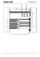
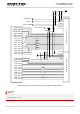
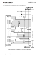
CSI2 data lines CSI1_LN2_P, CSI_LN2_N, CSI_LN3_P and CSI_LN3_N can be multiplexed into MIPI
signals for the fourth camera in four-camera application.
3.20.1. Design Considerations
Special attention should be paid to the pin definition of LCM/camera connectors. Assure the SC66
and the connectors are correctly connected.
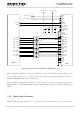
MIPI are high speed signal lines, supporting maximum data rate up to 2.1Gbps. The differential
impedance should be controlled as 85Ω. Additionally, it is recommended to route the trace on the
inner layer of PCB, and do not cross it with other traces. For the same group of DSI or CSI signals, all
the MIPI traces should keep the same length.
CSI/DSI should reference the ground at all times,ground cuts and voids in the path of CSI/DSI signals
should be avoided or removed.
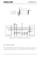
Route the camera CLK signal in the inner layer of the PCB between ground fills
Spacing of the Lanes according to the following rules:
a) intrapair p to n : 1*trace width
b) Lane to Lane : 1.5*trace width
c) to all other signals : 2.5*trace width
Route MIPI traces according to the following rules:
a) The CSI trace length should not exceed 170mm and the DSI trace length should not exceed
110mm;
b) Control the differential impedance as 85Ω±10%;
c) Control intra-lane length difference within 0.7mm;
d) Control inter-lane length difference within 1.4mm.
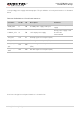
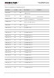
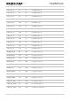
Table 28: MIPI Trace Length Inside the Module
Pin
Signal
length
Length(P-N)
116
DSI0_CLK_N
27.37
-0.10
115
DSI0_CLK_P
27.27
118
DSI0_LN0_N
27.03
0.04
117
DSI0_LN0_P
27.07
120
DSI0_LN1_N
26.65
-0.05
119
DSI0_LN1_P
26.60
122
DSI0_LN2_N
26.54
-0.01
NOTE