
Product Info


Smart LTE Module Series
SC66 Hardware Design
SC66_Hardware_Design 62 / 118
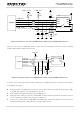
SD_CMD
120K
NM_51K
SD_DATA3
SD_DATA2
SD_CLK
SD_DATA0
SD_DET
SD_DATA1
P1-DAT2
P2-CD/DAT3
P3-CMD
P4-VDD
P5-CLK
P8-DAT1
GND
P6-VSS
P7-DAT0
DETECTIVE
GND
GND
GND
1
2
3
4
5
6
7
8
9
10
11
12
13
33R
33R
33R
33R
33R
33R
1K
33pF
4.7uF
Module
R1 R2
R3 R4
R5
R6
NM_51K
NM_10K
NM_51K
NM_51K
R7
R8
R9
R10
R11
R12
R13
D1 D2
D3
D4 D5
D6
D7
D8
C1
C2
SD Card Connector
LDO13A_1P8
SD_VDD
SD_PU_VDD
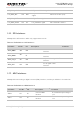
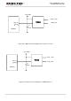
Figure 19: Reference Circuit for SD Card Interface
SD_VDD is a peripheral driver power supply for SD card. The maximum drive current is 600mA. Because
of the high drive current, it is recommended that the trace width is 0.5mm or above. In order to ensure the
stability of drive power, a 4.7uF and a 33pF capacitor should be added in parallel near the SD card
connector.
CMD, CLK, DATA0, DATA1, DATA2 and DATA3 are all high speed signal lines. In PCB design, please
control the characteristic impedance of them as 50Ω, and do not cross them with other traces. It is
recommended to route the trace on the inner layer of PCB, and keep the same trace length for CLK, CMD,
DATA0, DATA1, DATA2 and DATA3. CLK additionally needs ground shielding.
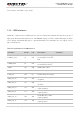
Layout guidelines:
Control impedance as 50Ω±10%, and ground shielding is required.
The difference in trace lengths among the clock, data, and command signals should be less than 2
mm.
The Bus length should be less than 100mm.
The spacing to all other signals and lane-to-lane should be at least one and a half times the line
width.
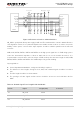
Table 19: SD Card Signal Trace Length Inside the Module
Pin No.
Signal
Length (mm)
Comment
70
SD_CLK
24.58
69
SD_CMD
24.32
68
SD_DATA0
24.33