
Product Info

Smart LTE Module Series
SC66 Hardware Design
SC66_Hardware_Design 58 / 118
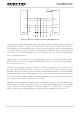
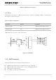
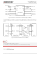
VCCA
VCCB
OE
A1
A2
A3
A4
GND
B1
B2
B3
B4
LDO11A_1P8
UART
6_ RTS
UART6_ RXD
UART
6_ CTS
UART6_ TXD
RXD_3.3V
CTS_3.3V
TXD_3.3V
VDD_3.3V
TXS0104EPWR
C1
100pF
C2
U1
100
pF
RTS_3.3V
Figure 15: Reference Circuit with Level Translator Chip (for UART6)
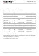
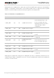
The following figure is an example of connection between SC66 and PC. A voltage level translator and a
RS-232 level translator chip are recommended to be added between the module and PC, as shown
below:
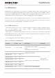
TXS0104 EPWR
RXD_3.3V
CTS_3.3V
VCCA
Module
GND
GND
1.8V
VCCB
3.3V
DIN 1
ROUT3
ROUT 2
ROUT1
DIN4
DIN3
DIN 2
DIN 5
FORCEON
3.3V
DOUT1
DOUT2
DOUT3
DOUT4
DOUT5
RIN3
RIN2
RIN1
VCC GND
OE
SN65C 3238
DB-9
RTS
TXD
CTS
RXD
GND
RTS_3.3V
UART6_TXD
UART6_RTS
UART6_RXD
UART6_CTS
TXD_1.8V
RTS_1.8V
RXD_1.8V
CTS_1.8V
/FORCEOFF
/INVALID
R1OUTB
TXD_3.3V
Figure 16: RS232 Level Match Circuit (for UART5)
1.DEBUG UART, UART1,LPI_UART_2 are similar to UART6. Please refer to UART6 reference circuit
design for DEBUG UART, UART1,LPI_UART_2.
2.LPI_UART_2 is a low power UART and it is not recommended for the time being.
3.11. (U)SIM Interfaces
NOTE