
Product Info

Smart LTE Module Series
SC66 Hardware Design
SC66_Hardware_Design 53 / 118
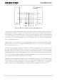
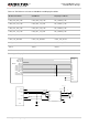
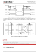
The following is a reference design for TYPE-C interface:
USB1_HS_DM
Module
USB
_
SS1
_RX_P
RX2+
RX2-
VBUS
CC1
D-
D+
TX2-
TX2+
CC2
USB_CC1
USB_CC2
RX1+
RX1-
TX1+
TX1-
USB Type-C
C6
C7
C8
C9
C10
C11
C12
C13
USB1_HS_DP
USB_VBUS
USB
_
SS1
_RX_M
USB
_
SS1
_TX_P
USB
_
SS1
_TX_M
USB
_
SS2
_RX_P
USB
_
SS2
_RX_M
USB
_
SS2
_TX_P
USB
_
_TX_M
SS2
B11
B10
A3
A2
B2
B3
A11
A10
UUSB_TYPEC
VPH_PWR
10K
SS_DIR_OUT
SS_DIR_IN
0R
Figure 12: USB Type-C Interface Reference Design
In order to ensure USB performance, please follow the following principles while designing USB interface.
It is important to route the USB signal traces as differential pairs with total grounding. The impedance
of USB differential trace is 90Ω.
The ground reference plane must be continuous,without any cuts or any holes under the USB
signals,to ensure impedance continuity.
Pay attention to the influence of junction capacitance of ESD protection devices on USB data lines.
Typically, the capacitance value should be less than 2pF for USB 2.0 and less than 0.5pF for USB 3.1.
besides.Keep the ESD protection devices as close as possible to the USB connector.
Do not route signal traces under crystals, oscillators, magnetic devices ,audio signal,and RF signal
traces. It is important to route the USB differential traces in inner-layer with ground shielding on not
only upper and lower layers but also right and left sides.
Keep USB3.1 signal routing away from RF signal. Crossing and parallel with RF signal line is
forbidden. The isolation between USB3.0 signal and RF signal should be more than 90 db. Otherwise,
it will interfere with RF signal strongly.
Make sure the trace length difference between USB 3.1 RX/TX differential pairs do not exceed
0.7mm.
Make sure the trace length difference between USB 2.0 DP/DM differential pairs do not exceed 2mm.