
Product Info

Smart LTE Module Series
SC66 Hardware Design
SC66_Hardware_Design 35 / 118
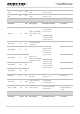
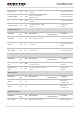
TP0_RST
138
DO
Reset signal of
touch panel (TP0)
V
OL
max=0.45V
V
OH
min=1.35V
1.8V power
domain. Active low.
TP0_INT
139
DI
Interrupt signal of
touch panel (TP0)
V
IL
max=0.63V
V
IH
min=1.17V
1.8V power
domain.
TP0_I2C_SCL
140
OD
I2C clock signal of
touch panel (TP0)
1.8V power
domain.
TP0_I2C_SDA
206
OD
I2C data signal of
touch panel (TP0)
1.8V power
domain.
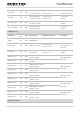
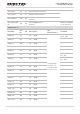
LCM Interfaces
Pin Name
Pin
No.
I/O
Description
DC Characteristics
Comment
PWM
152
DO
PWM Output
LCD0_RST
127
DO
LCD0 reset signal
V
OL
max=0.45V
V
OH
min=1.35V
1.8V power domain
It should not be
pulled up.
LCD0_TE
126
DI
LCD0 tearing
effect signal
V
IL
max=0.63V
V
IH
min=1.17V
1.8V power
domain.
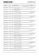
DSI0_CLK_N
116
AO
LCD0 MIPI clock
signal (negative)
85Ω differential
impedance.
DSI0_CLK_P
115
AO
LCD0 MIPI clock signal
(positive)
DSI0_LN0_N
118
AO
LCD0 MIPI lane 0 data
signal (negative)
85Ω differential
impedance.
DSI0_LN0_P
117
AO
LCD0 MIPI lane 0 data
signal (positive)
DSI0_LN1_N
120
AO
LCD0 MIPI lane 1 data
signal (negative)
85Ω differential
impedance.
DSI0_LN1_P
119
AO
LCD0 MIPI lane 1 data
signal (positive)
DSI0_LN2_N
122
AO
LCD0 MIPI lane 2 data
signal (negative)
85Ω differential
impedance.
DSI0_LN2_P
121
AO
LCD0 MIPI lane 2 data
signal (positive)
DSI0_LN3_N
124
AO
LCD0 MIPI lane 3 data
signal (negative)
85Ω differential
impedance.
DSI0_LN3_P
123
AO
LCD0 MIPI lane 3 data
signal (positive)
Camera Interfaces