
Product Info


LTE Module Series
EG25-G Mini PCIe Hardware Design
EG25-G_Mini_PCIe_Hardware_Design 25 / 48
Clock and mode can be configured by AT command, and the default configuration is master mode using
short frame synchronization format with 2048KHz PCM_CLK and 8KHz PCM_SYNC. In addition, EG25-G
Mini PCIe’s firmware has integrated the configuration on some PCM codec’s application with I2C interface.
Please refer to document [2] for details about AT+QDAI command.
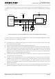
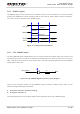
The following figure shows a reference design of PCM interface with an external codec IC.
PCM_DIN
PCM_DOUT
PCM_SYNC
PCM_CLK
I2C_SCL
I2C_SDA
Module
1.8V
4.7K
4.7K
BCLK
LRCK
DAC
ADC
SCL
SDA
BIAS
MICBIAS
INP
INN
LOUTP
LOUTN
Codec
Figure 9: Reference Circuit of PCM Application with Audio Codec
3.8. Control and Indicator Signals
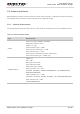
The following table shows the pin definition of control and indicator signals.
Table 10: Pin Definition of Control and Indicator Signals
Pin No.
Pin Name
I/O
Power Domain
Description
17
RI
DO
3.3V
Output signal to wake up the host.
31
DTR
DI
3.3V
Sleep mode control
20
W_DISABLE#
DI
3.3V
Airplane mode control; pull-up by default;
active low.
22
PERST#
DI
3.3V
Fundamental reset signal; active low.
42
LED_WWAN#
OC
LED signal for indicating the network
status of the module; active low
1
WAKE#
OC
Output signal to wake up the host.