
Product Info


LTE Module Series
EG25-G Mini PCIe Hardware Design
EG25-G_Mini_PCIe_Hardware_Design 22 / 48
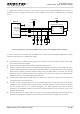
The following principles should be complied with when design the USB interface, so as to meet USB 2.0
specification.
It is important to route the USB signal traces as differential pairs with total grounding. The impedance
of USB differential trace is 90Ω.
Do not route signal traces under crystals, oscillators, magnetic devices and RF signal traces. It is
important to route the USB differential traces in inner-layer with ground shielding on not only upper
and lower layers but also right and left sides.
Pay attention to the influence of junction capacitance of ESD protection components on USB data
lines. Typically, the capacitance value should be less than 2pF.
Keep the ESD protection components as close to the USB connector as possible.
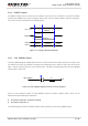
1. There are three preconditions when enabling EG25-G Mini PCIe to enter into the sleep mode:
a) Execute AT+QSCLK=1 command to enable the sleep mode. Please refer to document [2] for
details.
b) DTR pin should be kept at high level (pull-up internally).
c) USB interface on Mini PCIe must be connected with the USB interface of the host and please
guarantee the USB of the host is in suspension state.
2. “*” means under development.
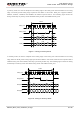
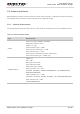
3.6. UART Interface
The following table shows the pin definition of the main UART interface.
Table 8: Pin Definition of Main UART Interface
The main UART interface supports 9600bps, 19200bps, 38400bps, 57600bps, 115200bps and
230400bps baud rates, and the default is 115200bps. This interface can be used for AT command
communication and data transmission.
Pin No.
Pin Name
I/O
Power Domain
Description
11
UART_RX
DI
3.3V
UART receive data
13
UART_TX
DO
3.3V
UART transmit data
23
UART_CTS
DI
3.3V
UART clear to send
25
UART_RTS
DO
3.3V
UART request to send
NOTES
S