
Product Info

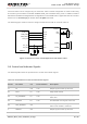


LTE Module Series
EG25-G Mini PCIe Hardware Design
EG25-G_Mini_PCIe_Hardware_Design 21 / 48
3.5. USB Interface
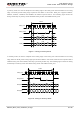
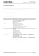
The following table shows the pin definition of USB interface.
Table 7: Pin Definition of USB Interface
EG25-G Mini PCIe is compliant with USB 2.0 specification. It can only be used as a slave device.
Meanwhile, it supports high speed (480Mbps) mode and full speed (12Mbps) mode. The USB interface is
used for AT command communication, data transmission, GNSS NMEA output, software debugging,
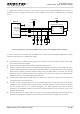
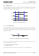
firmware upgrade and voice over USB*. The following figure shows a reference circuit of USB interface.
USB_DP
USB_DM
GND
USB_DP
USB_DM
GND
L1
Close to Module
R3
R4
Test Points
ESD Array
NM_0R
NM_0R
Minimize these stubs
Module
MCU
USB_VBUS
VDD
Figure 6: Reference Circuit of USB Interface
A common mode choke L1 is recommended to be added in series between the module and customer’s
MCU in order to suppress EMI spurious transmission. Meanwhile, the 0Ω resistors (R3 and R4) should be
added in series between the module and the test points so as to facilitate debugging, and the resistors are
not mounted by default. In order to ensure the integrity of USB data line signal, L1/R3/R4 components
must be placed close to the module, and also these resistors should be placed close to each other. The
extra stubs of trace must be as short as possible.
Pin No.
Pin Name
I/O
Description
Comment
36
USB_DM
IO
USB differential data (-)
Require differential impedance of 90Ω
38
USB_DP
IO
USB differential data (+)
Require differential impedance of 90Ω