
Product Info


LTE Module Series
EG25-G Mini PCIe Hardware Design
EG25-G_Mini_PCIe_Hardware_Design 18 / 48
1. Keep all NC, reserved and unused pins unconnected.
2.
1)
The digital audio (PCM) function is only supported on Telematics version.
3.3. Power Supply
The following table shows pin definition of VCC_3V3 pins and ground pins.
Table 5: Definition of VCC_3V3 and GND Pins
The typical supply voltage of EG25-G Mini PCIe is 3.3V. In the 2G network, the input peak current may
reach 2.7A during the transmitting time. Therefore, the power supply must be able to provide enough
current, and a bypass capacitor of no less than 470µF with low ESR should be used to prevent the
voltage from dropping.
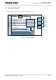
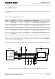
The following figure shows a reference design of power supply. The precision of resistor R2 and R3 is 1%,
and the capacitor C3 needs a low ESR.
LDO_IN
C1
C2
MIC29302WU U1
IN
OUT
EN
GND
ADJ
2 4
1
3
5
VCC_3V3
100nF
C3
470uF
C4
100nF
R2
82K 1%
47K 1%
R3
470uF
470R
51K
R4
R1
MCU_POWER
_ON/OFF
47K
4.7K
R5
R6
C5
C6
33pF
10pF
TVS
D1
Figure 3: Reference Circuit of Power Supply
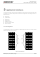
Pin No.
Pin Name
I/O
Power Domain
Description
2, 39, 41, 52
VCC_3V3
PI
3.0V~3.6V
3.3V DC supply
4, 9, 15, 18, 21,
26, 27, 29, 34, 35,
37, 40, 43, 50
GND
Mini card ground
NOTES