
Product Info


LTE Module Series
BG96 Hardware Design
BG96_Hardware_Design 63 / 81
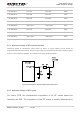
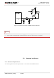
Figure 25: Coplanar Waveguide Line Design on a 4-layer PCB (Layer 3 as Reference Ground)
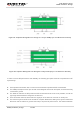
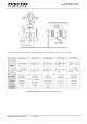
Figure 26: Coplanar Waveguide Line Designon a4-layer PCB (Layer 4 as Reference Ground)
In order to ensure RF performance and reliability, the following principles should be complied with in RF
layout design:
Use impedance simulation tool to control the characteristic impedanceof RF tracesas 50Ω.
The GND pins adjacent to RF pins should not bedesigned as thermal relief pads, and should be fully
connected to ground.
The distance between the RF pinsand the RFconnectorshould be as short as possible, and all the
right angle tracesshould be changed to curved ones.
There should be clearance area under the signal pin of the antenna connector or solder joint.
The reference ground of RF traces should be complete. Meanwhile, adding some ground viasaround
RF traces and the reference ground could help to improve RF performance. The distance between