
Product Info


LTE Module Series
BG96 Hardware Design
BG96_Hardware_Design 62 / 81
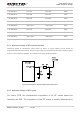
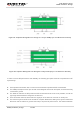
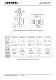
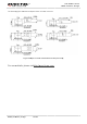
the trace width (W), the materials’ dielectric constant, the distance between
signal layer and reference ground (H), and the clearance between RF trace
and ground(S). Microstrip line or coplanar waveguide line is typically used in
RF layout for characteristic impedance control. The following are reference
designs of microstrip line or coplanar waveguide linewithdifferent PCB
structures.
Figure 23: Microstrip Line Designon a 2-layer PCB
Figure 24: Coplanar Waveguide Line Design on a 2-layer PCB