
Product Info


LTE Module Series
BG96 Hardware Design
BG96_Hardware_Design 61 / 81
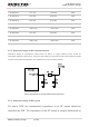
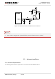
5.1.3. Reference Design of RF Antenna Interface
Areference design of mainantenna padis shown as below. A π-type matching circuit should be
reservedfor better RF performance, and the π-type matching components (R1/C1/C2) should be placed
as close to the antenna as possible. The capacitors are not mounted by default.
Figure 22: Reference Circuit of RF Antenna Interface
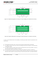
5.1.4. Reference Design of RF Layout
For user’s PCB, the characteristic impedance of all RF traces should be
controlled as 50Ω. The impedance of the RF traces is usually determined by
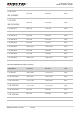
LTE-FDD B13 777~787 746~756 MHz
LTE-FDD B18 815~830 860~875 MHz
LTE-FDD B19 830~845 875~890 MHz
LTE-FDD B20 832~862 791~821 MHz
LTE-FDD B25 1850~1915 1930~1995 MHz
LTE-FDD B26 814~849 859~894 MHz
LTE-FDD B28 703~748 758~803 MHz
LTE-TDD B39 1880~1920 1880~1920 MHz