
Product Info

LTE Module Series
BG96 Hardware Design
BG96_Hardware_Design 54 / 81
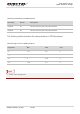
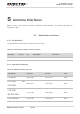
Table 20: Pin Definition of USB_BOOT Interface
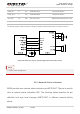
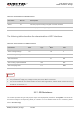
The following figure shows a reference circuit of USB_BOOT interface.
Figure 21: Reference Circuit of USB_BOOT Interface
It is recommended to reserve the above circuit design during application design.
3.16. ADC Interfaces
The module provides two analog-to-digital converter (ADC) interfaces.AT+QADC=0 command can be
used to read the voltage value on ADC0 pin. AT+QADC=1 command can be used to read the voltage
value on ADC1 pin. For more details about these AT commands, please refer todocument [2].
In order to improve the accuracy of ADCvoltage values, the trace of ADC should be surrounded by
ground.
Pin Name Pin No. I/O Description Comment
USB_BOOT 75 DI
Force the module to enter into
emergency download mode
1.8V power domain.
Active high.
If unused, keep it open.
NOTE