
Product Info

LTE Module Series
BG96 Hardware Design
BG96_Hardware_Design 47 / 81
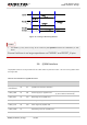
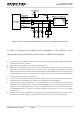
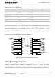
Table 11: Pin Definition of UART1Interface
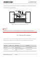
Table 12: Pin Definition of UART2Interface
Table 13: Pin Definition of UART3Interface
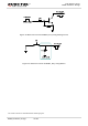
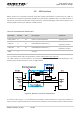
The logic levels are described in the following table.
Pin Name Pin No. I/O Description Comment
DTR 30 DI
Data terminal ready.
Sleepmode control
1.8V power domain
RXD 34 DI Receive data 1.8V power domain
TXD 35 DO Transmit data 1.8V power domain
CTS 36 DO Clear to send 1.8V power domain
RTS 37 DI Request to send 1.8V power domain
DCD 38 DO Data carrier detection 1.8V power domain
RI 39 DO Ring indicator 1.8V power domain
Pin Name Pin No. I/O Description Comment
DBG_RXD 22 DI Receive data 1.8V power domain
DBG_TXD 23 DO Transmit data 1.8V power domain
Pin Name Pin No. I/O Description Comment
UART3_TXD 27 DO Transmit data 1.8V power domain
UART3_RXD 28 DI Receive data 1.8V power domain