
Product Info

LTE Module Series
BG96 Hardware Design
BG96_Hardware_Design 44 / 81
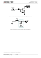
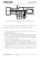
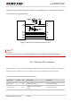
Figure 14: Reference Circuit of (U)SIM Interface with a 6-Pin (U)SIM Card Connector
In order to enhance the reliability and availability of the (U)SIM card in
applications, please follow the criteria below in (U)SIM circuit design:
Keep placement of (U)SIM card connector as close to the module as possible. Keep the trace length
as less than 200mm as possible.
Keep (U)SIM card signals away from RF and VBAT traces.
Assure the ground between the module and the (U)SIM card connector short and wide. Keep the
trace width of ground and USIM_VDD no less than 0.5mm to maintain the same electric potential.
Make sure the bypass capacitor between USIM_VDD and USIM_GND less than 1uF, and place it as
close to (U)SIM card connector as possible. If the system ground plane is complete, USIM_GND can
be connected to the systemground directly.
To avoid cross-talk between USIM_DATA and USIM_CLK, keep them awayfromeach other and
shield them with surrounded ground. USIM_RST should also be ground shielded.
In order to offer good ESD protection, it is recommended to add a TVSdiode array with parasitic
capacitance not exceeding15pF. In order to facilitate debugging, it is recommended to reserve series
resistors for the (U)SIM signals of the module.The 33pFcapacitors are used for filtering interference
of GSM900MHz.Please note that the (U)SIM peripheral circuit should be close to the (U)SIM
cardconnector.
The pull-up resistor on USIM_DATA line can improve anti-jamming capability when long layout trace
and sensitive occasion areapplied, and should be placed close to the (U)SIM cardconnector.